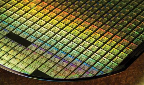
The End of Semiconductor Scorekeeping
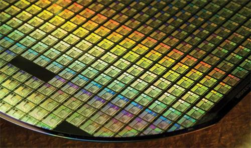
Why 2nm May Be the Last Technology Node With a Clear Winner
By Lucas Reinhardt
Senior Semiconductor Analyst
Last Updated: April 2, 2026
Reading Time: 9 min read
One of the hottest topics in the semiconductor industry in 2026 remains 2nm.
The media continues to debate TSMC's N2, Samsung's SF2, and Intel's 18A. Investors keep asking the same questions: Who is ahead? Who is behind? Who will win the next generation of advanced process technology?
The question sounds perfectly reasonable. After all, for more than two decades, the semiconductor industry has been a competition with a relatively clear scoreboard. The company with the most advanced node was usually the company that won.
But the 2nm era is revealing a new reality: even if every technical metric were publicly available, people might still struggle to answer a surprisingly simple question—who won 2nm?
The problem is not a lack of information.
The problem is that the method used to measure victory is beginning to break down.
Part I: When Process Nodes Were a Reliable Scoreboard
Looking back at the industry's history over the past two decades—from Intel's Tick-Tock era to TSMC's rise with 7nm and the widespread adoption of FinFETs—the industry relied on a simple assumption: smaller process nodes delivered higher transistor density, lower power consumption, and better performance. Therefore, process leadership generally translated into market leadership.
That logic worked for a long time because most customers in the CPU era were pursuing similar goals: higher performance, lower power consumption, and lower costs. The industry could operate under a shared evaluation framework. Winners and losers were relatively easy to identify. Semiconductor competition resembled a 100-meter sprint, with a finish line that everyone agreed upon.
According to technical documentation from IEEE Spectrum and Lam Research, semiconductor node names historically corresponded to actual physical dimensions. Around the 90nm generation in 2003, for example, the metal 1 half-pitch was approximately 90 nanometers.
However, technical references compiled by HandWiki point out that since roughly 1997, node names have no longer represented any specific physical dimension on a chip, whether gate length, metal pitch, or gate pitch.
In other words, by the time we arrived at "2nm," the number itself had already undergone nearly three decades of gradual transformation into a marketing label.
Part II: Process Node Names Are Losing Their Value as a Comparison Tool
In the past, nodes such as 90nm, 65nm, 45nm, and 28nm already contained some marketing influence, but the numbers still maintained a meaningful relationship with physical scaling.
Today, the situation is different. Intel 18A, TSMC N2, and Samsung SF2 are not identical technologies. They employ different design rules, prioritize different engineering objectives, and serve different customer requirements. The node labels still exist, but they are increasingly incapable of functioning as a universal scoring system.
According to TechInsights analyses presented around IEDM discussions, the three technologies show significant differences in transistor density:
- TSMC N2: approximately 313 MTr/mm² (high-density standard-cell implementation)
- Intel 18A: approximately 238 MTr/mm² according to TechInsights, while Intel's own estimates place it closer to 280 MTr/mm²
- Samsung SF2: approximately 231 MTr/mm²
Yet density is only one metric.
Intel 18A incorporates PowerVia backside power delivery, a feature absent from the initial version of TSMC N2. TSMC is expected to introduce backside power delivery later through its N2P variant after 2026.
According to TechInsights analysis cited by TechBriefly, Intel 18A achieved a performance score of 2.53, compared with 2.27 for TSMC N2 and 2.19 for Samsung SF2.
This creates an unusual situation:
TSMC leads in density. Intel leads in performance scoring. Samsung was first to commercialize Gate-All-Around (GAA) technology.
The result is that three different "2nm" technologies point toward three different definitions of leadership.
Part III: Why Nobody Can Agree on a Single Yield Number
One of the most common topics surrounding 2nm over the past several years has been yield.
Yet an interesting pattern has emerged: yield figures for the same process technology often change dramatically depending on when and where they are reported. Numbers published a few months apart can appear completely contradictory.
Many people assume someone must be wrong.
In reality, a more likely explanation is that people are often discussing entirely different metrics.
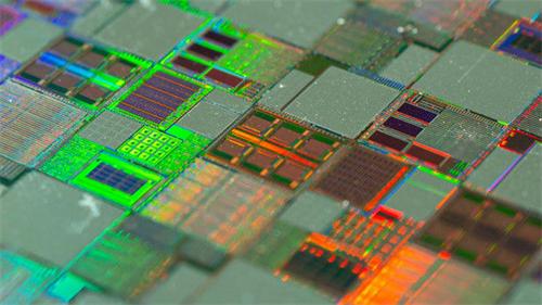
In the advanced-node era, the term "yield" may refer to several distinct measurements:
- SRAM Yield
- Logic Yield
- Full Chip Yield
- Risk Production Yield
- High-Volume Manufacturing Yield
Different reports may cite different definitions. As a result, the same process node can simultaneously have multiple "correct" yield figures.
Samsung's SF2 provides a useful example. KeyBanc estimated yields below 40% in mid-2025. DigiTimes later reported approximately 60% yield for Exynos 2600 production. TrendForce, using a stricter application-processor benchmark methodology, estimated yields closer to 50%.
The differences do not necessarily imply data manipulation.
Instead, they highlight a more fundamental issue: the evaluation standards themselves are different.
For investors and industry observers, the most important shift is not whether yields are high or low. The more significant change is that yield itself no longer has a universally accepted definition.
Once an industry loses agreement on how success should be measured, scorekeeping becomes increasingly difficult.
Part IV: Customers Are Beginning to Need Different Winners
In the past, customer requirements largely overlapped.
Today, that is no longer true.
For Apple, the most important considerations may be power efficiency, manufacturing consistency, and long-term supply reliability. SemiAnalysis has described Apple's relationship with TSMC as operating like "one team." Apple reportedly stations hundreds of engineers at TSMC facilities to collaborate on process design kits (PDKs) and manufacturing optimization.
This level of integration means Apple is not simply purchasing transistor density. It is purchasing predictable execution capability.
For NVIDIA, priorities may center on manufacturing extremely large dies, integrating HBM memory, and securing advanced packaging capacity. According to industry analysis from Oplexa, NVIDIA has already reserved a significant portion of TSMC's advanced CoWoS packaging capacity.
By 2026, CoWoS capacity is expected to expand from roughly 35,000 wafers per month at the end of 2024 to a target of approximately 130,000 wafers per month. Even at that scale, demand continues to exceed supply.
For NVIDIA, access to sufficient CoWoS capacity may matter more than the underlying wafer technology itself.
For Google and Amazon, the focus may be total cost of ownership (TCO), data-center efficiency, and the speed at which AI infrastructure can be deployed.
Reports indicate that Google even reduced its 2026 TPU production targets by roughly 25% due in part to CoWoS packaging constraints.
When different customers optimize for different outcomes, the same question can produce multiple correct answers.
The industry begins to shift from one market, one standard, one winner toward multiple markets, multiple standards, and multiple winners.
Part V: The Real Bottleneck Has Already Moved Beyond the Wafer Fab
Even as 2nm technology continues to advance, many of the industry's most important constraints are increasingly emerging elsewhere in the supply chain.
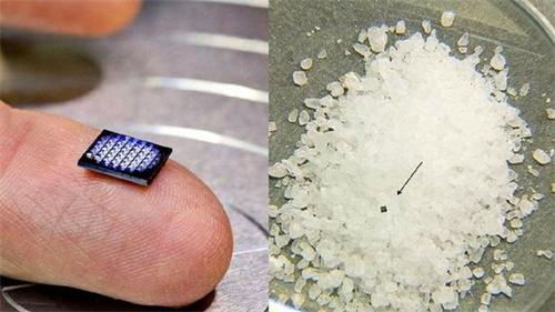
IBM Makes Chips 2nm Smaller Than Rice Granules
According to TrendForce analysis, the primary bottlenecks in the AI semiconductor ecosystem by 2026 have shifted away from wafer manufacturing and toward advanced packaging and High Bandwidth Memory (HBM).
TSMC's capital expenditure has reached approximately $56 billion in 2026, with a significant portion directed toward expanding advanced packaging technologies such as CoWoS and SoIC.
Today, the success of a leading-edge AI chip depends not only on wafer fabrication but also on:
- Chiplet design
- Packaging architecture (CoWoS, EMIB, Foveros)
- Memory bandwidth (HBM3E, HBM4)
- Software-stack optimization
Advanced process nodes remain important.
They simply no longer determine the outcome by themselves.
Part VI: The Semiconductor Industry Is Experiencing a Failure of the Scoring System
For decades, the industry relied on a shared scoreboard: process nodes, transistor counts, and clock frequencies. These metrics were often effective predictors of competitive success.
Today, semiconductor competition increasingly resembles cloud computing, AI platforms, and smartphone ecosystems.
The number of relevant evaluation dimensions continues to grow, and no single metric can adequately describe overall competitiveness.
This transformation is not unique to semiconductors.
University rankings, autonomous-driving classifications, and AI model leaderboards all face similar challenges. As systems become more complex, any single scoring methodology becomes increasingly distorted and incomplete.
Why might 2nm be the last technology node with a clearly identifiable winner?
Because advanced process technology will continue to evolve. After 1.4nm, there will almost certainly be additional nodes. What may disappear is the clear winner-take-all dynamic that characterized previous generations.
The industry is transitioning from a single-variable competition to a multi-variable ecosystem competition.
Conclusion: Competition Will Continue, but a Universal Winner May Not
For the past two decades, the semiconductor industry has largely been a contest centered on process technology.
People became accustomed to identifying first place, second place, and third place. A single number often appeared sufficient to determine who was winning.
2nm may represent the final moment when that mindset still feels intuitive.
Competition is not going away. But future competition may increasingly resemble cloud computing, AI models, and smartphone ecosystems, where different technological approaches serve different needs and different customers choose different answers.
When that transition is complete, what disappears is not advanced process technology.
What disappears is the scoring system the industry has relied on for decades.
Data Sources
Key data and industry references cited in this article are drawn from the following organizations and publications: TechInsights (transistor density analysis), TrendForce (market-share and capacity data), SemiAnalysis (customer collaboration and ecosystem analysis), Oplexa (advanced packaging bottleneck analysis), and IEEE Spectrum, Lam Research, and HandWiki (historical discussions of process-node naming conventions).
All yield figures referenced are analyst estimates and industry assessments. Variations across sources are intentional examples illustrating one of the article's central arguments: that yield itself no longer has a universally accepted definition.
Lucas Reinhardt
Senior Semiconductor Analyst
Lucas Reinhardt is a semiconductor industry analyst focused on advanced manufacturing, memory technologies, and AI infrastructure. His work explores how supply chains, fabrication technologies, and capital investment decisions reshape the global computing landscape. Before becoming an independent analyst, he spent years covering the European semiconductor ecosystem and industrial technology markets.
Recommended for you