The HBM4 Bottleneck
Why Memory Is Emerging as the Critical Constraint in NVIDIA's AI Stack
By Lucas Reinhardt
Senior Semiconductor Analyst
Last Updated: June 2, 2026
Reading Time: 14 min read
For many cloud providers and AI model developers, purchasing an NVIDIA platform is no longer simply a matter of buying GPUs. Behind every new generation of AI accelerators lies an increasing amount of high-bandwidth memory, advanced packaging capacity, and complex supply-chain resources. In the past, memory was an important component sitting beside the chip. Today, it is increasingly becoming the key constraint that determines how quickly an entire AI system can scale. HBM4 is one of the clearest manifestations of this shift.
Part I: Why the AI Industry Has Suddenly Started Paying Attention to Memory
The Hidden Assumption Behind GPU Performance Growth
Over the past decade, the semiconductor industry has become accustomed to attributing performance improvements to more advanced process nodes, higher transistor counts, and more powerful compute units. AI workloads, however, have a unique characteristic: computational capability only matters if data can be supplied continuously.
As model parameter counts grow, model weights become larger, context windows expand, and multimodal data becomes more complex, the volume of data that GPUs must process is growing at a pace that is beginning to approach—or even exceed—the growth rate of compute performance. This means AI expansion now requires not only more computation, but also faster data movement.
From a Compute Race to a Bandwidth Race
To understand this transition, it is important to distinguish among three metrics: FLOPS (floating-point computing capability), memory bandwidth, and memory capacity.
All three are important during AI training. During AI inference—particularly autoregressive decoding—the situation changes. In the decoding phase, only one token is generated at a time, yet the entire model's weights must be read from memory. As a result, the upper limit of inference performance is no longer determined by FLOPS, but by memory bandwidth.
According to a deployment guide published by Spheron Network in May 2026, for inference of a 70B-parameter model with a batch size of one, the theoretical TPS limit is approximately 24 on the H100 (HBM3, 3.35 TB/s), approximately 34 on the H200 (HBM3E, 4.8 TB/s), and approximately 57 on the B200 (HBM3E, 8.0 TB/s). These upper limits are determined by memory bandwidth rather than FLOPS.[1]
Academic research has further reinforced this conclusion. A survey on Agentic AI inference published on arXiv in April 2026 found that from NVIDIA Ampere to Blackwell, the I/O-to-compute ratio declined by a factor of 14.4, indicating that memory-bandwidth growth has significantly lagged compute growth.[1] Another paper published in April 2025 demonstrated a 2.15× improvement in attention-kernel efficiency on NVIDIA H20 GPUs through asynchronous KV-cache prefetching, directly showing that HBM bandwidth has become a primary bottleneck in modern LLM inference.[1]
Part II: Why HBM4 Has Become a Critical Constraint
The Evolution of HBM: From Supporting Actor to Leading Role
HBM has already gone through multiple generations of evolution. HBM2e was used in the A100, HBM3 in the H100, and HBM3E in the H200 and Blackwell series. In April 2025, JEDEC released the HBM4 standard (JESD270-4). Two changes stand out. First, the external interface widened from 1,024 bits to 2,048 bits, doubling the data channels. Second, the base die responsible for communication is now manufactured using logic processes.[2]
According to Siemens Semiconductor Packaging's technical guide published in April 2026, HBM4 supports per-pin speeds ranging from 6.4 to 12.8 Gbps, delivering more than 2.0 TB/s of bandwidth per stack and up to 3.3 TB/s in advanced configurations. Capacity scales up to 64 GB per stack with 16-layer stacking. Core voltage drops from 1.1V to 1.05V, while energy efficiency improves by roughly 60% compared with HBM2 and HBM2E.[2]
The Changing Role of HBM in NVIDIA's Product Roadmap
NVIDIA's product lineup clearly illustrates how HBM has evolved from a supporting component into a defining part of the product itself.
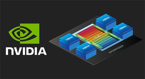
NVIDIA SOD Chiplet Architecture Diagram with HBM4 Memory & Interposer
The H100 integrates 80 GB of HBM3 with 3.35 TB/s of bandwidth. The H200 upgrades this to 141 GB of HBM3E with 4.8 TB/s. The Blackwell B200 uses 192 GB of HBM3E and delivers 8.0 TB/s. With the arrival of the Vera Rubin R100, the configuration jumps to 288 GB of HBM4 and an astonishing 22 TB/s of total bandwidth.[3] In an Agentic AI environment characterized by exploding context lengths, HBM3E's approximately 8 TB/s bandwidth is increasingly inadequate for handling KV-cache bottlenecks. Rubin's 22 TB/s suggests that the location of the bottleneck itself is shifting.
Why Expanding HBM Production Is Far More Difficult Than Expanding GPU Production
HBM is not ordinary DRAM. It is closer to a hybrid of advanced logic chips and memory chips.
Manufacturing HBM requires Through-Silicon Via (TSV) technology, which vertically connects dozens of wafer layers with micron-level precision. Twelve-layer stacks are already in mass production, while sixteen-layer stacks are now being developed. According to a June 2026 report from TechPowerUp, Samsung's HBM4 design presented at ISSCC 2026 combines sixth-generation 10nm-class (1c) DRAM core dies with an SF4 logic base die. TSV counts have increased fourfold, enabling operating speeds of up to 13 Gbps per pin.[3]
Samsung's decision to use SF4 for the base die, however, comes at a significantly higher cost than competing approaches. SK hynix uses TSMC's N12 logic process, while Micron relies on its own CMOS base-die technology, both of which are more cost-effective solutions.[3] As a result, the HBM4 race is not only a technological competition but also a contest of cost structures.
Sixteen-Layer Stacking: The Manufacturing Hell Behind a Single Number
The leap from twelve layers to sixteen layers is far more difficult than the transition from eight layers to twelve.
According to TrendForce in January 2026, sixteen-layer HBM requires wafers to be thinned to roughly 30 microns, compared with around 50 microns for current twelve-layer designs. With JEDEC limiting HBM4 package height to 775 microns, traditional manufacturing methods are approaching their physical limits.[4]
SK hynix employs the MR-MUF process, which simultaneously heats and interconnects all vertically stacked dies, offering higher efficiency than the TC-NCF layer-by-layer stacking methods used by Samsung and Micron. Samsung, meanwhile, is betting on hybrid bonding technology and aims to commercialize sixteen-layer HBM4E products by 2028. According to Sisa Journal, Samsung has already supplied hybrid-bonding HBM4 prototypes to major customers, including NVIDIA, but current yields are only around 10%.[4]
Part III: The Real Bottleneck Is Not the Chip—It Is the System
Blackwell Is Not a GPU; It Is a System
Many people still think of a GPU as a standalone chip. In reality, modern AI platforms have evolved into systems composed of GPUs, HBM, packaging technologies, and networking infrastructure.
Take NVIDIA Blackwell as an example. A single B200 package contains two compute dies connected through NVLink-HBI, surrounded by HBM3E stacks and integrated on a CoWoS-L substrate. Without CoWoS packaging, these dies would remain isolated pieces of silicon rather than a functional product.
According to an April 2026 analysis by Oplexa, TSMC's CoWoS capacity is expected to grow from approximately 35,000 wafers per month at the end of 2024 to roughly 130,000 wafers per month by the end of 2026—nearly quadrupling in less than two years—yet demand still exceeds supply. TSMC CEO C.C. Wei has publicly acknowledged that CoWoS capacity remains "extremely tight" and that 2026 capacity is fully booked.[5]
How HBM Affects the Entire AI Infrastructure Stack
The effects of HBM supply constraints propagate through a long chain.
The first impact is on GPU delivery schedules. According to Next Waves Insight in May 2026, approximately 70% of the HBM4 used in NVIDIA's Vera Rubin platform comes from SK hynix, around 25% from Samsung, and only a single-digit percentage from Micron. The 2026 HBM output of all three suppliers has already been committed through multi-year agreements. The market is no longer governed by price discovery but by administrative allocation.[6]
The second impact is on supplier dynamics. One noteworthy detail is that Micron's HBM4 samples reportedly exceed 11 Gbps, outperforming SK hynix's approximately 10 Gbps samples. Yet Micron's share of Vera Rubin's HBM4 supply remains in the single digits. This suggests that NVIDIA's supplier selection criteria extend beyond peak performance and include production scale, supply reliability, and the depth of long-term partnerships. These factors collectively form the hidden barriers of the HBM market.
When HBM supply is constrained, GPU shipments are constrained as well, disrupting AI infrastructure expansion plans at cloud providers. Google has reportedly reduced its 2026 TPU production target from approximately four million units to roughly three million units—a reduction of about 25%—due to limitations in CoWoS packaging capacity.[5]
The third impact is on AI training costs. According to Silicon Analysts data from April 2026, HBM4 costs approximately $520 per stack compared with roughly $330 per stack for HBM3E, representing an increase of more than 50%. TrendForce expects HBM4 to account for the majority of HBM industry revenue by the end of 2026.[7]
Part IV: If Memory Is So Important, Why Doesn't NVIDIA Manufacture HBM Itself?
NVIDIA Controls the AI Platform, But Not HBM Manufacturing
NVIDIA is one of the most influential companies in AI computing, yet it does not manufacture HBM. The reason is not that NVIDIA lacks the desire to do so. Rather, the barriers to entry in the HBM industry are extraordinarily high and difficult for new entrants to replicate.
Where the Real Barriers in the HBM Industry Exist
The first barrier is DRAM expertise. At its core, HBM is built from DRAM dies, and DRAM manufacturing requires decades of accumulated process knowledge. Samsung, SK hynix, and Micron collectively control the overwhelming majority of the global DRAM market. This concentration is not accidental; it is the result of massive capital investment and long-term yield-learning curves.
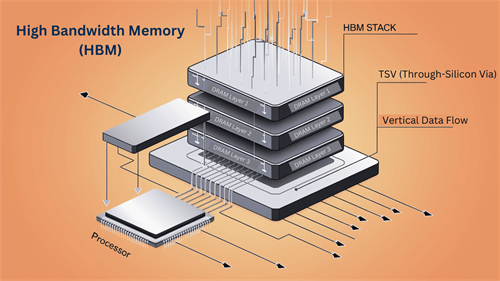
HBM DRAM Vertical Stack Structure & Processor Connection Schematic
The second barrier is manufacturing experience. TSV stacking, micro-bump bonding, thermal management, and related technologies all require extensive trial-and-error optimization. According to The Tech Room in April 2026, SK hynix encountered power-delivery challenges while developing twelve-layer HBM4 samples. Although the issue was ultimately resolved, it illustrates how even industry leaders are operating on a razor's edge.[7]
The third barrier is capital investment and industrial policy. Both Samsung and SK hynix are constructing dedicated HBM manufacturing facilities. Samsung's P5 factory is expected to become operational in 2028, while SK hynix's M15X facility is scheduled to begin operations in mid-2027. According to Data Center Dynamics in June 2026, SK hynix plans to increase infrastructure investment by more than four times, while Samsung aims to expand HBM production capacity by approximately 50%. These investments are further supported by South Korean government policies, including tax incentives, R&D subsidies, and export support measures, all of which raise barriers for potential new entrants.[8]
The fourth barrier is the yield-learning curve. HBM yield depends not only on the quality of individual DRAM dies but also on the reliability of the stacked structure as a whole. Sixteen-layer stacking means that a defect in any single layer can potentially compromise the entire stack. This cumulative risk makes yield improvement significantly slower than in conventional DRAM manufacturing.
Importance Does Not Necessarily Translate Into Control
HBM is becoming increasingly important, but that does not necessarily mean control of the industry will shift to memory manufacturers.
NVIDIA controls CUDA, system architecture, and platform standards, while HBM vendors control critical resources. This is a classic platform-versus-supplier relationship.
NVIDIA secures HBM supply through long-term agreements, influences the direction of HBM development through specification requirements, and controls final system integration through CoWoS packaging capabilities. In the third quarter of 2025, NVIDIA reportedly raised the HBM4 performance requirement for the Rubin platform to more than 11 Gbps, forcing suppliers to redesign die architectures and delaying volume production from the original 2025 timeline into the first quarter of 2026 and beyond.[5]
HBM vendors possess scarce resources, but their customer base is highly concentrated. According to eCorpIT's June 2026 analysis, NVIDIA consumes approximately 68% of global HBM output.[8] This asymmetrical dependence limits the pricing power and allocation flexibility of memory suppliers.
Part V: What HBM4 Reveals About the New Competitive Logic of the AI Industry
The AI Industry Is Entering a Multi-Bottleneck Era
In the past, GPUs were the primary bottleneck. Today, bottlenecks are spreading across multiple layers, including HBM, CoWoS packaging, networking interconnects, power delivery, and cooling infrastructure.
According to Oplexa, the combined AI infrastructure capital expenditures of the four largest cloud providers—Microsoft, Google, Amazon, and Meta—will reach approximately $650 billion in 2026, representing year-over-year growth of 71%.[5] At this scale of investment, shortages in any single supply-chain segment can affect the delivery capacity of the entire system.
Why Future Competition Increasingly Resembles Supply-Chain Competition
Competition in advanced AI systems is no longer solely about chip design. It is increasingly about who can coordinate the entire supply chain.
NVIDIA's advantage lies not only in GPU architecture but also in its ability to secure CoWoS capacity from TSMC, sign multi-year agreements with all three HBM suppliers, and build a networking ecosystem around NVLink and InfiniBand. This system-level integration capability is far more difficult to replicate than any single technical metric.
In June 2026, SK hynix and NVIDIA announced a multi-year technology partnership focused on advancing memory technologies for AI factories. Following the announcement, Jensen Huang publicly urged SK hynix to "produce more HBM chips." This seemingly paradoxical situation—a platform provider urging its supplier to expand production—perfectly illustrates HBM's central role in today's AI supply chain.[8]
The Semiconductor Industry's Evaluation Framework Is Changing
In the past, the industry asked questions such as: Who has the most advanced process node? Whose GPU is the fastest?
In the future, the questions may become: Who can secure critical resources? Who can scale entire systems? Who can guarantee supply-chain stability?
HBM4 accelerates this shift. When memory bandwidth becomes the decisive factor in inference performance, when HBM supply becomes a prerequisite for GPU shipments, and when CoWoS packaging becomes essential for transforming silicon into deployable products, the standard for evaluating an AI chip company is no longer the number of transistors it can place on a chip. It is the company's ability to mobilize and coordinate an entire supply chain.
Conclusion: The Most Important Thing About HBM4 Is Not How Fast It Is
Many people view HBM4 simply as another memory upgrade.
From an industry perspective, however, HBM4 represents something much larger: the core constraint in AI competition is shifting from the performance of individual chips to the ability of entire systems to move data efficiently.
HBM4 may not ultimately become the single defining bottleneck of the AI industry. CoWoS packaging, power infrastructure, and network bandwidth are all competing for that distinction. Nevertheless, HBM4 has already emerged as one of the clearest examples of where the industry is heading. It demonstrates that in the AI era, system performance is often determined not by the most powerful component, but by the scarcest constraint.
And that may ultimately be the true battleground on which NVIDIA, SK hynix, Micron, and Samsung are competing.
References
- Spheron Network. (2026). HBM3e vs HBM4 vs HBM4e for LLM inference: GPU memory bandwidth decision guide; arXiv. (2026). Networking-aware energy efficiency in agentic AI inference: A survey (arXiv:2604.07857v1); arXiv. (2025). Accelerating LLM inference throughput via asynchronous KV cache prefetching (arXiv:2504.06319).
- JEDEC Solid State Technology Association. (2025). JESD270-4: High bandwidth memory 4 (HBM4); Siemens Digital Industries Software. (2026, April). HBM3e and HBM4: IC design guide for next-generation high bandwidth memory. Siemens Semiconductor Packaging.
- SemiAnalysis. (2026, June). ISSCC 2026: NVIDIA and Broadcom CPO, HBM4 & LPDDR6. SemiAnalysis Newsletter; TechPowerUp. (2026, June 13). TSMC unveils next-generation HBM4 base dies, built on 12 nm and 5 nm nodes.
- TrendForce. (2026, January). NVIDIA fuels HBM4 race: 12-layer ramps, 16-layer push by SK hynix, Samsung, and Micron. TrendForce Research.
- Oplexa. (2026, April). AI chip packaging bottleneck: TSMC crisis 2026. Oplexa Market Intelligence.
- Next Waves Insight. (2026, May). HBM4 ramp: Why three suppliers still add up to a duopoly for Nvidia. Next Waves Insight.
- Silicon Analysts. (2026). Foundry allocation dashboard. Silicon Analysts; The Tech Room. (2026, April). SK Hynix holds 62% HBM crown as Micron overtakes Samsung — 2026 battle pivots to HBM4.
- Data Center Dynamics. (2026, June). Samsung and SK Hynix to scale up memory production capacity in 2026. Data Center Dynamics; eCorpIT. (2026, June). SK Hynix Nvidia AI factories deal explained. eCorpIT.
Lucas Reinhardt
Senior Semiconductor Analyst
Lucas Reinhardt is a semiconductor industry analyst focused on advanced manufacturing, memory technologies, and AI infrastructure. His work explores how supply chains, fabrication technologies, and capital investment decisions reshape the global computing landscape. Before becoming an independent analyst, he spent years covering the European semiconductor ecosystem and industrial technology markets.
Recommended for you