The End of Easy Scaling in NAND
Why 400 Layers May Matter Less Than the Rules They Rewrite
By Lucas Reinhardt
Senior Semiconductor Analyst
Last Updated: June 8, 2026
Reading Time: 14 min read
For two decades, NAND scaling meant stacking more layers.
At 400 layers, that rule may no longer work.
In 2026, Samsung is fighting three wars at once.
In the HBM market, it is chasing SK hynix, whose market share has already reached roughly 54% to 62%, while Samsung holds around 35% to 40%. In DRAM, it faces slowing growth as wafer capacity and capital spending increasingly shift toward HBM. In NAND, margins remain under long-term pressure, yet moving to 400 layers requires entirely new investments: construction of the Pyeongtaek P4 production line, procurement of wafer-to-wafer bonding equipment, and development of BV NAND processes. Each of these demands enormous amounts of capital.
Yet at precisely this moment, Samsung has chosen to commit to something even more complicated—and far less certain in terms of returns—than HBM: 400-layer NAND.
It is not an easy decision to understand. From a financial perspective, NAND margins are nowhere near HBM margins. From a technology-risk perspective, 400-layer NAND requires skipping intermediate nodes and moving directly to a completely new wafer-to-wafer bonding architecture, and its production timeline has already experienced delays. From a competitive perspective, SK hynix's 321-layer QLC NAND entered mass production first in August 2025, with a 375-layer product targeted for late 2026—a roadmap that appears stable and predictable.
So why, at the very moment Samsung most needs to prove itself in HBM, does it still believe that next-generation NAND deserves this level of investment?
The answer may be that, for Samsung, 400-layer NAND is not merely a product. It is a strategic statement.
For most of the past decade, Samsung was the unquestioned leader in both DRAM and NAND. But in 2026, Samsung finds itself under pressure on every front simultaneously: SK hynix is leading in HBM, DRAM growth is slowing, and NAND profitability remains weak. At such a moment, abandoning leadership in 400-layer NAND would amount to publicly admitting that Samsung can no longer define all three major trajectories of the memory industry at the same time.
As a result, 400-layer NAND becomes a demonstration.
A demonstration that Samsung can still fight on multiple fronts simultaneously.
A demonstration that it remains capable of defining the next generation of memory standards.
1. The Trap of the Number
Throughout the history of NAND flash, nearly every new generation has been described as a "historic turning point."
People said it at 96 layers.
They said it again at 176 layers.
They said the same thing at 232 layers and 286 layers.
This time, however, the situation is fundamentally different.
From 96 layers to 286 layers, manufacturers were essentially doing the same thing: stacking more memory cells vertically. Through better etch technology and process optimization, each generation became taller and denser than the previous one.
This was fundamentally a process optimization problem.
Whoever had the better etch tools, more precise deposition equipment, and stronger yield management could build higher stacks.
The transition from 286 layers to 400 layers is different.
The challenge is no longer simply building a taller structure.
The marginal returns from straightforward vertical stacking are approaching zero.
According to reporting by TechPowerUp citing The Korea Economic Daily, Samsung's tenth-generation V-NAND (V10) will adopt an entirely new architecture known as BV NAND (Bonded Vertical NAND). In this architecture, the memory cell array and peripheral control circuitry are no longer manufactured on the same wafer. Instead, they are fabricated separately on different wafers and then connected through wafer-to-wafer (W2W) bonding technology. The resulting bit density may increase by approximately 1.6 times, or 60%, while interface speeds are expected to improve as well.
What does this actually mean?
It means NAND manufacturing is moving from process optimization to system-level architectural reconstruction.
Manufacturers no longer need to manage a single wafer process flow. They must simultaneously manage two separate wafer processes, followed by highly precise wafer bonding.
Manufacturing complexity is no longer increasing along one dimension. It is expanding across an entire system.
It is also worth noting that Samsung did not invent W2W bonding.
According to AllPCB, Samsung has signed a patent licensing agreement with China's Yangtze Memory Technologies (YMTC) covering hybrid bonding technology and will adopt a technology path similar to Xtacking beginning with V10. YMTC introduced Xtacking more than four years ago. By manufacturing peripheral circuitry and memory arrays separately before bonding them together, Xtacking can reduce chip area by approximately 25% and shorten product development cycles by roughly three months.
As a result, the truly significant development is not the number "400."
What matters is that reaching it requires the industry to abandon the rules that governed NAND scaling for the past two decades.
2. Not Replacement, but Parallel Investment
A common misconception is that Samsung faces a simple resource-allocation dilemma between HBM and NAND.
This view is too linear.
Within Samsung, resource allocation is not a straightforward substitution problem. HBM teams and NAND teams rely on different technical expertise, different equipment ecosystems, and different customer bases. Moving NAND budget into HBM does not automatically accelerate Samsung's progress in HBM.
A more accurate interpretation is this:
At the very moment Samsung most needs to prove itself in HBM, it continues investing heavily in next-generation NAND because NAND represents something strategically irreplaceable.
The concern is not financial optimization.
It is strategic relevance.
What happens if Samsung abandons leadership in 400-layer NAND?
First, SK hynix's gradual roadmap—321 layers already in production and 375 layers on the way—would be validated as the "correct" approach, while Samsung's aggressive strategy would be viewed as excessive risk-taking.
Second, YMTC's Xtacking platform has already demonstrated that wafer-to-wafer bonding is commercially viable. If Samsung fails to participate, it risks losing influence over the architectural standards that may define future NAND generations.
Third, equipment suppliers such as Lam Research, Tokyo Electron (TEL), and Applied Materials are beginning to reorganize competitive positions around wafer bonding and cryogenic etching technologies. If Samsung remains absent from that transition, it risks losing influence over critical parts of the supply chain.
This concern is not hypothetical.
According to TrendForce, Samsung reduced its 2026 NAND wafer target from 4.9 million wafers to 4.68 million wafers annually, while SK hynix lowered its target from 1.9 million wafers to 1.7 million wafers. Both companies are deliberately tightening supply to support pricing.
Yet Samsung continues investing in 400-layer NAND production at Pyeongtaek P4.
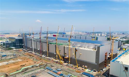
Samsung NAND Flash Facility (credit: Samsung Global Newsroom)
This combination—shrinking legacy capacity while funding a new architecture—reflects something more than financial calculation.
It reflects a strategic commitment.
Even if NAND is no longer the most profitable memory business, Samsung cannot afford to lose the ability to define its future.
3. The Deepening Supply Chain
Once NAND moves from process optimization to architectural reconstruction, the list of winners and losers changes.
And this time, the biggest winners may not be NAND manufacturers at all.
How do W2W bonding and BV NAND change the barriers to entry?
Previously, NAND competition centered on a simple question:
Who has the best etch technology?
Now the question becomes:
Who can successfully manage two wafer process flows plus high-precision bonding?
That shift fundamentally changes the role of equipment suppliers.
They are no longer simply selling tools.
They are increasingly selling customized solutions tied directly to specific architectures.
Consider cryogenic etching.
This is one of the critical technologies enabling 400-layer NAND. It performs etching under extremely low temperatures to maintain stability in ultra-high-aspect-ratio structures.
According to SemiEngineering, Lam Research introduced its third-generation cryogenic etching platform, Lam Cryo 3.0, in July 2024. The company reports that approximately 1,000 cryogenic etch chambers have already been installed across NAND production lines worldwide.
TEL introduced its first cryogenic etch platform in 2023 and claims its new technology can etch structures equivalent to more than 400 layers while operating 2.5 times faster than conventional approaches.
Lam Research currently holds a leading position in this segment.
TEL, however, is advancing rapidly.
According to Nikkei Asia, TEL expects its 400-layer-class technologies to be adopted within the next two to three years.
This means Samsung's equipment decisions for V10 involve more than technical specifications.
They involve supply-chain strategy.
Choosing Lam means extending existing relationships.
Choosing TEL could provide more favorable technology terms or faster equipment availability.
Why does equipment selection become a strategic issue?
Because suppliers are no longer delivering individual tools.
They are providing integrated solutions deeply intertwined with BV NAND manufacturing flows.
The competition between Lam Research and TEL is ultimately a competition over who can better support Samsung's W2W bonding architecture.
The same logic applies to materials.
Four-hundred-layer NAND is expected to require molybdenum (Mo) as a replacement for traditional tungsten (W) word-line materials because tungsten's electrical resistance increasingly becomes a bottleneck at higher layer counts.
That transition will reshape the upstream materials ecosystem.
As a result, one of the least discussed questions in NAND today is this:
Whether Samsung's BV NAND, SK hynix's hybrid-bonding strategy, or YMTC's Xtacking architecture ultimately prevails, equipment suppliers may emerge as the most consistent beneficiaries.
The pattern resembles what has happened in HBM.
In HBM, GPU vendors do not necessarily capture the greatest economic value. Companies such as TSMC, which control critical advanced-packaging capabilities, have gained some of the strongest bargaining power in the ecosystem.
NAND may be moving in the same direction.
As architectural complexity exceeds the capabilities of any single manufacturer, critical supply-chain participants—including equipment suppliers, materials vendors, and packaging providers—will gain more influence than they possessed during the previous decade.
4. What Samsung Is Really Betting On
By investing in 400-layer NAND, Samsung is effectively betting on one thing:
That AI-driven storage demand will not disappear as quickly as previous NAND demand cycles.
To understand that wager, it helps to place it in historical context.
In 2010, the rise of smartphones created unprecedented demand for NAND.
Many believed mobile devices would permanently break NAND's traditional boom-and-bust cycles.
Samsung, Micron, and SK hynix expanded aggressively.
By 2015 and 2016, oversupply had emerged and NAND prices collapsed.
In 2017, data-center expansion generated another surge in demand.
Cloud storage, big-data analytics, and streaming media appeared to offer a durable long-term growth trajectory.
Manufacturers expanded capacity again.
By 2019, another oversupply cycle arrived.
In 2021, pandemic-driven remote work and online entertainment pushed NAND demand even higher.
Supply-chain disruptions combined with work-from-home demand to drive NAND prices to new highs.
Then, in 2022 and 2023, consumer-electronics demand weakened sharply and the NAND market entered another downturn.
Each time, the market declared:
"This time is different."
Each time, the cycle returned.
In 2026, AI is creating an entirely new category of enterprise storage demand.
A single AI server rack, such as NVIDIA's NVL72 platform, may require more than one petabyte of NAND capacity.
Agentic AI systems and retrieval-augmented generation (RAG) workloads are increasing demand for high-IOPS, low-latency enterprise SSDs, transforming enterprise flash storage from an optional component into essential infrastructure.
Yet Samsung's investment in 400 layers is not a prediction about how long AI demand will last.
It is a bet on something else.
It is a bet that even if the cycle returns, Samsung must still possess the next generation of technology.
This is an offensive move rooted in defense.
If AI demand continues, Samsung's 400-layer technology may provide an advantage in enterprise SSD markets.
If AI demand eventually follows the same cyclical pattern as previous NAND markets, Samsung will at least avoid falling behind SK hynix or YMTC in terms of technological capability.
In other words, Samsung is not betting that AI will eliminate NAND cycles.
It is betting that, regardless of whether those cycles disappear, technological leadership remains the only viable survival strategy.
5. Redefining Leadership
If the race toward 400-layer NAND produces a winner, that winner may not be a company.
It may be a new definition of competition itself.
Samsung and SK hynix are pursuing fundamentally different paths.
SK hynix is following an incremental strategy.
Its 321-layer QLC NAND entered mass production in August 2025.
Its 375-layer product is targeted for late 2026.
Products beyond 400 layers remain part of a longer-term roadmap.
The advantages of this approach are stability, predictability, and manageable risk.
Every step includes clear technical validation and a defined production timeline.
According to reporting by icspec citing ETNews, SK hynix is also developing wafer-to-wafer hybrid-bonding technology, although its pace of adoption appears significantly more cautious than Samsung's.
Samsung, by contrast, is pursuing an aggressive strategy.
Rather than progressing through intermediate nodes such as 300 layers and 350 layers, it intends to move directly from 286 layers to a V10 generation exceeding 400 layers.
The advantage is the possibility of creating an immediate technology gap.
The downside is that any delay in technology validation or production ramp-up carries greater consequences.
Samsung's V9 QLC product, for example, was delayed until the first half of 2026 because of design-related issues.
Traditional analysis would frame this as a binary outcome:
If Samsung succeeds...
If Samsung fails...
But reality is usually more complicated than consulting-slide scenarios.
A more interesting possibility is that both companies succeed simultaneously while defining leadership in entirely different ways.
Samsung may successfully define the architectural standards of next-generation NAND—BV NAND, wafer-to-wafer bonding, molybdenum word lines, and related technologies—establishing the technical benchmark for future generations.
However, if production schedules slip again or initial yields and costs prove challenging, those advantages may not translate into market leadership until 2027.
SK hynix, meanwhile, may continue demonstrating stronger execution and profitability.
Its 321-layer product is already shipping.
Its 375-layer generation is approaching.
Customer deliveries remain reliable.
Margins remain healthy.
Yet if Samsung's 400-layer architecture ultimately proves superior, SK hynix may eventually need to accelerate its own transition toward wafer-bonded architectures, accepting higher technical risks and capital requirements.
History offers many examples of this separation between technology definers and market executors.
Intel defined the x86 architecture.
AMD achieved faster growth during certain periods.
Nokia accumulated enormous technological expertise and patent portfolios in mobile devices.
Apple redefined the smartphone market.
The most likely future, therefore, may not be one winner and one loser.
Instead, the industry may begin evaluating leadership through multiple lenses.
For Samsung, leadership may mean defining the technical standards of next-generation NAND.
For SK hynix, leadership may mean delivering the products customers need on a predictable timeline.
These definitions are not mutually exclusive.
But they represent fundamentally different competitive logics.
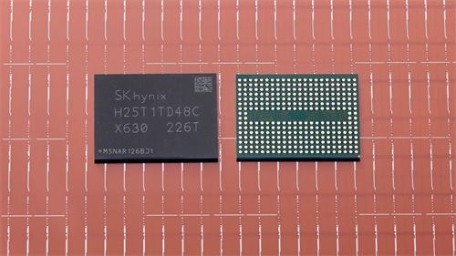
SK Hynix Races Samsung to 400+ Layer NAND
Conclusion: A Question Without an Answer
Four-hundred-layer NAND is not the answer.
It is merely the right question.
What happens when NAND can no longer rely on straightforward layer scaling to create competitive advantage?
Will the industry fragment into multiple technology camps—wafer-to-wafer bonding, hybrid bonding, Xtacking, and other architectures pursuing separate paths?
Or will competition increasingly become a test of capital intensity, where only companies such as Samsung, SK hynix, and Micron possess the financial resources required for architectural reconstruction while second-tier players gradually exit?
Regardless of whether Samsung's 400-layer strategy succeeds or fails, it marks the end of an era.
The era of easy scaling in NAND is coming to a close.
For the past two decades, the industry's greatest advantage was that everyone knew where the road led.
Stack more layers.
Buy better etch tools.
Optimize manufacturing processes.
The path was expensive, but it was clear.
Today, the question is whether the industry still shares the same roadmap.
The next phase will be more expensive, more complex, and more uncertain.
In that world, the ability to define the rules may become more valuable than the ability to manufacture the products.
And the rules themselves may not have been written yet.
Sources
- Counterpoint Research, Global NAND Memory Market Surges to a Record $46B in Q1 2026 as AI Demand Drives Massive Growth (June 2, 2026)
- TrendForce, Combined Revenue of Top Five Global NAND Flash Suppliers Rose by 83.7% QoQ for 1Q26 as Supply Shortages Drove Price Hikes (May 25, 2026)
- TechPowerUp / Korea Economic Daily, Samsung Plans 400-Layer V-NAND for 2026 and DRAM Technology Advancements by 2027 (October 29, 2024)
- AllPCB, 3D NAND Hits 400+ Layers with Hybrid Bonding (August 27, 2025)
- SK hynix Official Newsroom, 2026 Market Outlook: SK hynix's HBM to Fuel AI Memory Boom (April 24, 2026)
- Notebookcheck / SK hynix Statement, SK hynix Sells Out DRAM, NAND, and HBM Chip Supply Through 2026 (October 30, 2025)
- Unibetter IC, NAND Shortage 2026 Guide: Price and Market Outlook Analysis (March 31, 2026)
- SemiEngineering, Cryogenic Etch: A Key Enabler of 3D NAND (April 21, 2026)
Lucas Reinhardt
Senior Semiconductor Analyst
Lucas Reinhardt is a semiconductor industry analyst focused on advanced manufacturing, memory technologies, and AI infrastructure. His work explores how supply chains, fabrication technologies, and capital investment decisions reshape the global computing landscape. Before becoming an independent analyst, he spent years covering the European semiconductor ecosystem and industrial technology markets.
Recommended for you